Difference between revisions of "Computer architecture for software developers"
m |
|||
| (29 intermediate revisions by one other user not shown) | |||
| Line 1: | Line 1: | ||
| + | [[Category:HPC-Developer]] | ||
== Introduction == | == Introduction == | ||
| Line 29: | Line 30: | ||
As a consequence of its clocked operation a single clock cycle is a common time unit within processors. | As a consequence of its clocked operation a single clock cycle is a common time unit within processors. | ||
| + | |||
| + | ==== Consequences for software developers ==== | ||
| + | |||
| + | For benchmarking scaling behaviour the frequency has to be fixed to separate influences the impact of different clock frequencies and parallel scaling. For performance modelling the actual frequency (which may be lower as the nominal clock in case of SIMD) has to be taken into account. In any case it is recommended to measure the actual frequency while benchmarking with a HPM counter tool. | ||
=== Instruction level parallelism === | === Instruction level parallelism === | ||
| − | Stored program computers process a sequential instruction stream, the order of the instructions is fixed. Already early in computer history (1956, IBM 7030) computers exploited the opportunity to execute instruction in parallel. It is till today a main technology to generate higher performance. A prerequisite for instruction level parallelism is that there are enough independent instructions in the sequential instruction stream. The common metric for quantifying instruction throughput is CPI (cycles per instruction) or its inverse IPC (instructions per cycle). Instruction level parallelism works best for repetitive code sequences (loop structures). | + | Stored program computers process a sequential instruction stream, the order of the instructions is fixed. Already early in computer history (1956, IBM 7030) computers exploited the opportunity to execute instruction in parallel. The assumption is that there are independent instructions that can be executed concurrently. It is till today a main technology to generate higher performance. A prerequisite for instruction level parallelism is that there are enough independent instructions in the sequential instruction stream. The common metric for quantifying instruction throughput is CPI (cycles per instruction) or its inverse IPC (instructions per cycle). Instruction level parallelism works best for repetitive code sequences (loop structures). Typical values for CPI for real application codes is anything between 0.4 to 1 (in average two to one instructions throughput per cycle). |
==== Instruction pipelining ==== | ==== Instruction pipelining ==== | ||
| Line 44: | Line 49: | ||
==== Supporting technologies ==== | ==== Supporting technologies ==== | ||
| − | Instruction level parallelism can be controlled by hardware or by software. Modern processors typically rely on hardware control. Because typical application codes expose very limited instruction level parallelism if executed in order and/or have only few instructions between jumps to other instruction addresses | + | Instruction level parallelism can be controlled by hardware or by software. Modern processors typically rely on hardware control. Because typical application codes expose very limited instruction level parallelism if executed in order and/or have only few instructions between jumps to other instruction addresses supporting techniques are required to be able to exploit more parallelism from a sequential instruction stream. |
* Out-of-order execution: Special hardware analysis a fixed instruction window in the instructions stream and may execute instructions out of order. | * Out-of-order execution: Special hardware analysis a fixed instruction window in the instructions stream and may execute instructions out of order. | ||
| Line 51: | Line 56: | ||
=== Memory hierarchy === | === Memory hierarchy === | ||
| + | |||
| + | A stored program computer in its simplest form only has one unified memory. Early it turned out, that instruction execution capabilities increase much faster than data transfer capabilities. Early on there were concepts to deploy smaller, faster memory, closer to a processor core. The main motivation is that one can wither build a small and fast memory or a large but slow memory. On the software side the application has to expose temporal data access locality. Caches only result in performance increases if the application frequently accesses a subset of the total data. The first known implementation of a data cache is on the IBM System/360 Model 85 (1968). Modern processor have multi-level cache hierarchies exposing complex topologies. For multi-level caches the term memory hierarchy is used. Other data paths as e.g. file or network IO may also be seen as a part of this memory hierarchy. | ||
| + | |||
| + | Data path capabilities are quantified by data access latency, this is the time you have to wait if you request a data item until you can use it, and bandwidth, the maximum amount of data you can transfer per time. | ||
| + | |||
| + | Illustration of typical data paths with their latency and bandwidth: | ||
| + | [[File:MemoryHierarchy.png|600px]] | ||
| + | |||
| + | Data is transferred between memory hierarchy levels in blocks of data, called cachelines. Cacheline sizes are typically 64b or 128b. Through this optimisation one has to pay the latency cost only once per cacheline, all accesses within the same block are served from the cache. This is also called temporal data access locality. | ||
| + | |||
| + | ==== Consequences for software developers ==== | ||
=== Simultaneous multithreading === | === Simultaneous multithreading === | ||
| − | === Data parallel execution units (SIMD) === | + | To increase the utilisation of execution resources processors are able to execute multiple instructions streams (hardware threads) sharing execution units and cache hierarchy of a single core. To enable simultaneous multithreading (SMT) registers set and control unit are duplicated. Multiple threads give the instruction scheduler more independent instructions to exploit pipelining and superscalar execution. An application must be threaded to benefit or there must be many applications running in throughput mode. Typical processors offer 2-way to 4-way SMT. The benefit depends on how many execution slots are not utilised by one instruction stream alone, and may be from no benefit to 30%, in extreme cases a factor (frequent pipelining hazards). |
| + | |||
| + | Comparison of standard vs. 2-way SMT core: | ||
| + | [[File:SMT-comparison.png|800px]] | ||
| + | |||
| + | ==== Consequences for software developers ==== | ||
| + | |||
| + | === Data parallel execution units === | ||
| + | |||
| + | Single instruction, multiple data (SIMD) is a class of parallel computers in Flynn's taxonomy, where a single instruction operates on multiple data operands simultaneously. This is usually implemented using wide SIMD registers, that can hold multiple operands. The slots within a SIMD register are often called register lanes. The assumption to the code is that the same operations are executed on a large number of independent operands. The implementation of SIMD in modern processors is often referred to as short-vector SIMD, where a SIMD register is between 16b and 64b wide. The register can hold as many operands as fit into the register width for the data type used. For double precision floating point numbers this results in 2 operands for 16b wide registers to eight operands for 64b wide registers. SIMD applies to arithmetic as well as load/store of data. To fully benefit from the SIMD feature it must be possible to load and store data in blocks of the SIMD width. From an architecture point of view SIMD is easy to integrate into an existing architecture as the instruction throughput is not altered, still each instruction does more work (operations). Of course SIMD puts more pressure on the memory hierarchy in terms of data throughput demands. As it turns out the wires required to connect the SIMD registers to the execution units generate a lot of heat and require that for wide SIMD the cores have to clocked down to stay within the TDP limits. SIMD is introduced to an existing instruction set architecture as instruction set extensions, additional instructions understood by the hardware. Most modern processors architectures support 16b SIMD (called SSE on X86 processors, VSX on Power and Neon on ARM), the 32b x86 SIMD extension is called AVX and is supported on AMD and Intel processors, 64b SIMD AVX512 and only supported on Intel processors. | ||
| + | |||
| + | SIMD was besides multicore a main driver for processor performance from 2005 to 2018. SIMD is still an important factor in the product that determines the core performance, but it is unlikely it is a driver for performance in the future. | ||
| + | |||
| + | ==== Consequences for software developers ==== | ||
=== Putting it all together === | === Putting it all together === | ||
| + | |||
| + | The primary goal on the core level is to ensure a constant instruction execution stream utilising all available execution slots. For floating point performance the number of operations per instruction is maximised by introducing data parallel instructions as well as special purpose instructions as fused-multiply add operation in a single instruction. | ||
| + | |||
| + | The single core floating point performance is computed by the following product: | ||
| + | |||
| + | [[File:Performance core.png|500px]] | ||
| + | |||
| + | For a Skylake processor with two FP FMA execution units <math>n^\text{FP}_\text{super}=2</math> and <math>n_\text{FMA}=2</math> and <math>n_\text{SIMD}=8</math> for double precision FP operations and using a AVX512 frequency of 1.9 GHz this results in a performance of 60.8 GF/s for a single core. This is an impressive performance, but if one misses out on one of the factors the performance drop is large. The serial performance not using FMA and SIMD is 7.6 GF/s (already accounting for the higher core frequency without SIMD), a performance level that is not different from cores 10 years ago. For the chip or node level performance the core count is simply multiplied with the single core performance. | ||
| + | |||
| + | In the following we will look on the simplified real core architecture of the Intel Skylake processor. Modern X86 processors deviate from the standard stored program computer design by having dedicated L1 caches for instructions and data. Such a separate memory for code and data is called Harvard architecture. Furthermore many architecture decode the instructions as fetched from memory into smaller so called uops. This is for example necessary for x86 where almost any instruction may contain a memory reference, for which a separate load has to be created. Also in X86 instructions have a varying length which makes it necessary to scan the fetched instruction code for instruction boundaries first. All this is done in a part of the core called front end. The front end on Skylake can deliver up to 6 uops per cycle to the scheduler for execution. The front end also contains a special cache for already decoded uops called loop stream buffer. The front end is rarely a bottleneck in HPC applications. | ||
| + | |||
| + | Next is the scheduler that is responsible to maximise the utilisation of execution slots by dynamically finding independent instructions that can be executed in a pipelined superscalar fashion. To do so the scheduler can hold an instruction window with 224 entries. While x86 with AVX512 has access to 16 integer and 32 FP registers there are many more so called shadow registers (180 integer and 168 FP in case of Skylake) for register renaming to break up false dependency chains and allow for out-of-order execution. | ||
| + | |||
| + | |||
| + | Simplified illustration of the Intel Skylake core architecture: | ||
| + | [[File:Skylake-architecture.png|800px]] | ||
== Node architecture == | == Node architecture == | ||
| Line 65: | Line 110: | ||
=== Node topology === | === Node topology === | ||
| + | |||
| + | [[File:Node-architecture.png|600px]] | ||
== System architecture == | == System architecture == | ||
| + | [[File:System-architecture.png|600px]] | ||
== Links and further information == | == Links and further information == | ||
* John Hennessy David Patterson: [https://www.elsevier.com/books/computer-architecture/hennessy/978-0-12-811905-1 Computer Architecture] - A Quantitative Approach. Still the standard text book on computer architecture | * John Hennessy David Patterson: [https://www.elsevier.com/books/computer-architecture/hennessy/978-0-12-811905-1 Computer Architecture] - A Quantitative Approach. Still the standard text book on computer architecture | ||
Latest revision as of 15:18, 3 September 2019
Introduction
Modern computers are still build following the "Stored Program Computing" design. The idea for stored program computers originates in the second world war, first working systems where build in the late fourties. Several earlier innovations enabled this machine: the idea of a universal Turing machine (1936), Claude E. Shannon's Master thesis on using arrangements of relays to solve Boolean algebra problems (1937) and Konrad Zuse anticipated in two patent applications that machine instructions could be stored in the same storage used for data (1936).
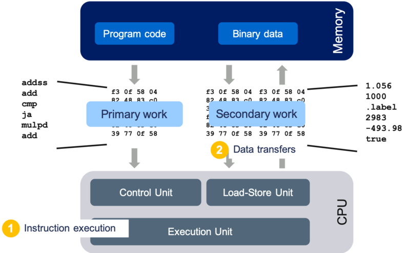
A stored program computer is controlled by instructions, the set of instructions a computer supports is also called instruction set architecture (ISA). Instructions are elementary operations as adding two numbers, loading data from memory or jumping to another location in the program code. Instructions are just integer numbers and are stored in a unified memory that also holds the actual data used by a program. A program consists of a sequential stream of instructions loaded from memory that control the hardware. The primary resource (or work) of a computer is therefore instruction execution. Some of those instructions load or store data from memory. To transfer data from memory is therefor a secondary resource of a computer triggered by instruction execution. The reason why this design was so successful lies in its generic application to any problem and the possibility to switch very fast between different applications. Everything in a computer is built of switches and as a consequence all numbers are represented in binary format. Because switches only know two states the operation of a computer is strictly clocked running with a certain fixed frequency. This generic nature of using a programmable machine together with extreme miniaturisation of the hardware enabled the application of computers in all aspects of our life.
Memory is organised in a linear fashion using so called addresses, integer numbers to reference a specific memory location. As the basic unit 8 bits also called a byte is used.
Illustration of Stored Program Computers:
The generic nature of stored program computers is also their biggest problem when it comes to speeding up execution of program code. As a program code can be any mix of supported instructions the properties of software and how it interacts with the hardware can vastly differ. Computer architects have chosen a pragmatic approach to speed up execution: "Make the common case fast". They analyse the software that runs on a computer and come up with improvements for this class of software. This also means that every hardware improvement makes assumptions against the software. Since chips are designed by profit-oriented companies other influences have to be considered as, e.g. technical opportunities as well as economical and marketing concerns.
In the following computer architecture is explained on a level that is relevant for software developers to understand the interaction of their software with the hardware.
Core architecture
Clock frequency
To increase the performance by increasing the clock frequency is the basic way of speeding up a stored program computer. Everything works faster and all codes will benefit. This was the main driver for performance until 2005. The ability to increase the frequency is strongly connected to instruction level parallelism techniques (see later). Why vendors are not able anymore to increase the frequency has multiple reasons but at the end it boils down to the physical limitation to dissipate the heat a chip generates with reasonable technical effort.
While clock frequency increase is not a main driver anymore it is still a technique employed in different ways. On one hand as one of two features (core count being the second) to rank of a processors according to price and on the other hand in form of the dynamic overclocking feature apparent in all modern processors.
Processors already support to dynamically decrease the clock to save power for a long time. Newer multicore processors in addition are capable of dynamically overclocking beyond the nominal frequency. On Intel processors this feature is called "turbo mode". Turbo mode is a flavour of so called "dark silicon" optimisations. A chip has a thermal design power (TDP). The TDP is the maximum heat the chip can dissipate. The power a chip consumes depends on the frequency and the square of the voltage it is operated with and of course the total number of transistors and wires active. There is a minimum voltage the chip can be operated with using a given frequency. If not all cores are used, parts of the chip can be turned off. This gives enough power headroom to increase the voltage and frequency and still stay within the TDP. The overclocking happens dynamically and is controlled by the hardware itself.
Many technological advances in processor designs are targeted on managing to stay within the TDP and still reach high performance. This is reflected in different clock domains for cores and uncore and special SIMD width specific turbo mode clocks. If a code uses wider SIMD units more transistors and more important wires are active, and the chip can therefore only run at a lower peak frequency.
As a consequence of its clocked operation a single clock cycle is a common time unit within processors.
Consequences for software developers
For benchmarking scaling behaviour the frequency has to be fixed to separate influences the impact of different clock frequencies and parallel scaling. For performance modelling the actual frequency (which may be lower as the nominal clock in case of SIMD) has to be taken into account. In any case it is recommended to measure the actual frequency while benchmarking with a HPM counter tool.
Instruction level parallelism
Stored program computers process a sequential instruction stream, the order of the instructions is fixed. Already early in computer history (1956, IBM 7030) computers exploited the opportunity to execute instruction in parallel. The assumption is that there are independent instructions that can be executed concurrently. It is till today a main technology to generate higher performance. A prerequisite for instruction level parallelism is that there are enough independent instructions in the sequential instruction stream. The common metric for quantifying instruction throughput is CPI (cycles per instruction) or its inverse IPC (instructions per cycle). Instruction level parallelism works best for repetitive code sequences (loop structures). Typical values for CPI for real application codes is anything between 0.4 to 1 (in average two to one instructions throughput per cycle).
Instruction pipelining
In instruction pipelining the execution of instructions is split into a series of sequential steps. Very similar to pipelining in car manufacturing this enables to work on different instruction in the different stages at the same time. The execution of an instruction is decomposed into smaller steps which enables to increase the clock frequency the pipeline is operated with. The execution of every single instruction still takes the same time but as soon as the pipeline is full every single cycle an instruction is finished. How many cycles it takes to execute one single instruction is the instruction latency while the total number is the instruction throughput. The optimal throughput for a single pipeline is one instruction per cycle (CPI=1).
Superscalar execution
Superscalar execution is the second major implementation of instruction level parallelism. Essentially the hardware can execute more than one instruction per cycle. The first superscalar processor was introduced shortly after the first pipelined processor in 1966 (CDC 6600). A superscalar processor has multiple execution units which can be active in the same cycle. The optimal throughput is a number larger than one. Typical implementations in modern processors are 4-way superscalar (CPI=0.25).
Supporting technologies
Instruction level parallelism can be controlled by hardware or by software. Modern processors typically rely on hardware control. Because typical application codes expose very limited instruction level parallelism if executed in order and/or have only few instructions between jumps to other instruction addresses supporting techniques are required to be able to exploit more parallelism from a sequential instruction stream.
- Out-of-order execution: Special hardware analysis a fixed instruction window in the instructions stream and may execute instructions out of order.
- Branch prediction: There is hardware support or guessing the outcome of branches based on previous occurrences.
- Speculative execution: On branches the predicted path is already fetched and executed before the actual outcome is known. If a branch was miss-predicted execution has to be rolled-back and repeated.
Memory hierarchy
A stored program computer in its simplest form only has one unified memory. Early it turned out, that instruction execution capabilities increase much faster than data transfer capabilities. Early on there were concepts to deploy smaller, faster memory, closer to a processor core. The main motivation is that one can wither build a small and fast memory or a large but slow memory. On the software side the application has to expose temporal data access locality. Caches only result in performance increases if the application frequently accesses a subset of the total data. The first known implementation of a data cache is on the IBM System/360 Model 85 (1968). Modern processor have multi-level cache hierarchies exposing complex topologies. For multi-level caches the term memory hierarchy is used. Other data paths as e.g. file or network IO may also be seen as a part of this memory hierarchy.
Data path capabilities are quantified by data access latency, this is the time you have to wait if you request a data item until you can use it, and bandwidth, the maximum amount of data you can transfer per time.
Illustration of typical data paths with their latency and bandwidth:
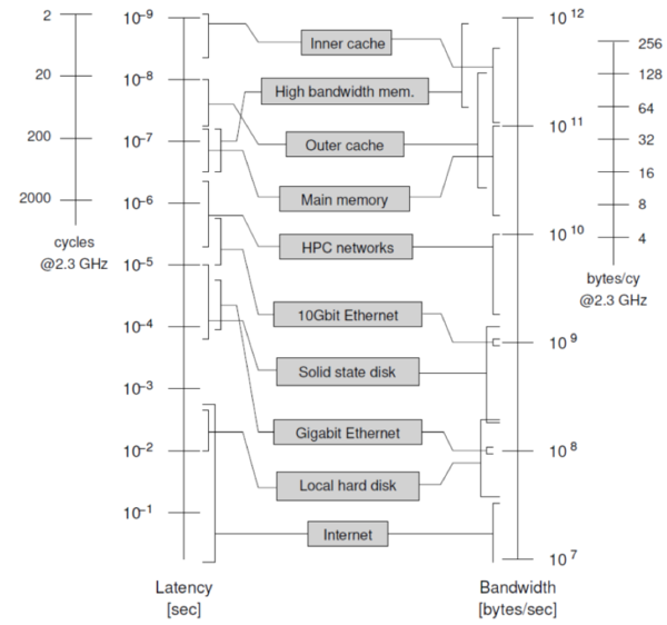
Data is transferred between memory hierarchy levels in blocks of data, called cachelines. Cacheline sizes are typically 64b or 128b. Through this optimisation one has to pay the latency cost only once per cacheline, all accesses within the same block are served from the cache. This is also called temporal data access locality.
Consequences for software developers
Simultaneous multithreading
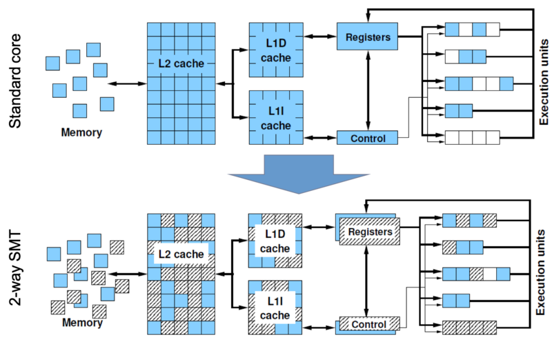
To increase the utilisation of execution resources processors are able to execute multiple instructions streams (hardware threads) sharing execution units and cache hierarchy of a single core. To enable simultaneous multithreading (SMT) registers set and control unit are duplicated. Multiple threads give the instruction scheduler more independent instructions to exploit pipelining and superscalar execution. An application must be threaded to benefit or there must be many applications running in throughput mode. Typical processors offer 2-way to 4-way SMT. The benefit depends on how many execution slots are not utilised by one instruction stream alone, and may be from no benefit to 30%, in extreme cases a factor (frequent pipelining hazards).
Comparison of standard vs. 2-way SMT core:
Consequences for software developers
Data parallel execution units
Single instruction, multiple data (SIMD) is a class of parallel computers in Flynn's taxonomy, where a single instruction operates on multiple data operands simultaneously. This is usually implemented using wide SIMD registers, that can hold multiple operands. The slots within a SIMD register are often called register lanes. The assumption to the code is that the same operations are executed on a large number of independent operands. The implementation of SIMD in modern processors is often referred to as short-vector SIMD, where a SIMD register is between 16b and 64b wide. The register can hold as many operands as fit into the register width for the data type used. For double precision floating point numbers this results in 2 operands for 16b wide registers to eight operands for 64b wide registers. SIMD applies to arithmetic as well as load/store of data. To fully benefit from the SIMD feature it must be possible to load and store data in blocks of the SIMD width. From an architecture point of view SIMD is easy to integrate into an existing architecture as the instruction throughput is not altered, still each instruction does more work (operations). Of course SIMD puts more pressure on the memory hierarchy in terms of data throughput demands. As it turns out the wires required to connect the SIMD registers to the execution units generate a lot of heat and require that for wide SIMD the cores have to clocked down to stay within the TDP limits. SIMD is introduced to an existing instruction set architecture as instruction set extensions, additional instructions understood by the hardware. Most modern processors architectures support 16b SIMD (called SSE on X86 processors, VSX on Power and Neon on ARM), the 32b x86 SIMD extension is called AVX and is supported on AMD and Intel processors, 64b SIMD AVX512 and only supported on Intel processors.
SIMD was besides multicore a main driver for processor performance from 2005 to 2018. SIMD is still an important factor in the product that determines the core performance, but it is unlikely it is a driver for performance in the future.
Consequences for software developers
Putting it all together
The primary goal on the core level is to ensure a constant instruction execution stream utilising all available execution slots. For floating point performance the number of operations per instruction is maximised by introducing data parallel instructions as well as special purpose instructions as fused-multiply add operation in a single instruction.
The single core floating point performance is computed by the following product:
For a Skylake processor with two FP FMA execution units and and for double precision FP operations and using a AVX512 frequency of 1.9 GHz this results in a performance of 60.8 GF/s for a single core. This is an impressive performance, but if one misses out on one of the factors the performance drop is large. The serial performance not using FMA and SIMD is 7.6 GF/s (already accounting for the higher core frequency without SIMD), a performance level that is not different from cores 10 years ago. For the chip or node level performance the core count is simply multiplied with the single core performance.
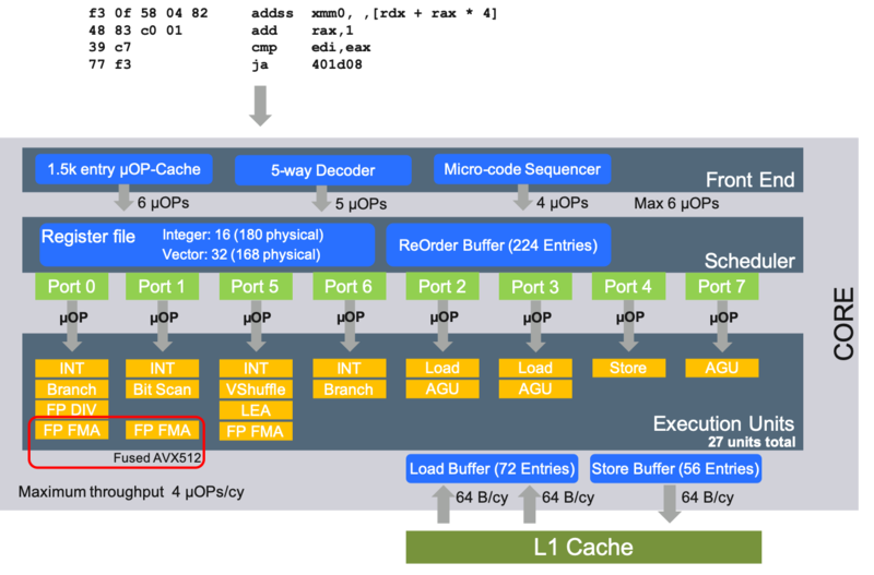
In the following we will look on the simplified real core architecture of the Intel Skylake processor. Modern X86 processors deviate from the standard stored program computer design by having dedicated L1 caches for instructions and data. Such a separate memory for code and data is called Harvard architecture. Furthermore many architecture decode the instructions as fetched from memory into smaller so called uops. This is for example necessary for x86 where almost any instruction may contain a memory reference, for which a separate load has to be created. Also in X86 instructions have a varying length which makes it necessary to scan the fetched instruction code for instruction boundaries first. All this is done in a part of the core called front end. The front end on Skylake can deliver up to 6 uops per cycle to the scheduler for execution. The front end also contains a special cache for already decoded uops called loop stream buffer. The front end is rarely a bottleneck in HPC applications.
Next is the scheduler that is responsible to maximise the utilisation of execution slots by dynamically finding independent instructions that can be executed in a pipelined superscalar fashion. To do so the scheduler can hold an instruction window with 224 entries. While x86 with AVX512 has access to 16 integer and 32 FP registers there are many more so called shadow registers (180 integer and 168 FP in case of Skylake) for register renaming to break up false dependency chains and allow for out-of-order execution.
Simplified illustration of the Intel Skylake core architecture:
Node architecture
Multicore chips
Cache-coherent non-uniform memory architecture (ccNUMA)
Node topology
System architecture
Links and further information
- John Hennessy David Patterson: Computer Architecture - A Quantitative Approach. Still the standard text book on computer architecture
